
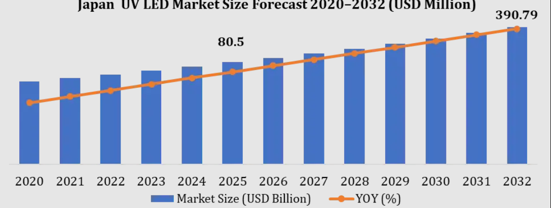
Japan UV LED Market Enters Accelerated Growth Phase, Forecasted to Reach USD 268.45 Million by 2032 with a Powerhouse 26.4% CAGR
The global landscape for optoelectronics and industrial semiconductor components is shifting rapidly toward sustainability, precision automation, and solid-state efficiency. At the forefront of this industrial transformation stands the Japan UV LED Market, which is officially entering an explosive, high-growth trajectory. According to a highly comprehensive strategic market intelligence report released by Maximize Market Research, the Japan UV LED market was valued at USD 51.5 Million in 2025 and is mathematically modeled to expand to an impressive USD 268.45 Million by 2032. This exponential surge represents a remarkable compounding annual growth rate (CAGR) of 26.4% during the forecast window spanning 2026 to 2032.
This massive surge is heavily supported by Japan's world-renowned precision manufacturing infrastructure, pioneering domestic semiconductor R&D, stringent eco-compliance mandates, and an accelerating nationwide transition away from hazardous conventional systems. As a critical subsystem provider within modern industrial ecosystems, UV LED technology is rapidly replacing obsolete mercury vapor lamp-based setups. It offers commercial operators a combination of minimal thermal emission, structural compactness, instant-on functionality, and drastically prolonged functional operational cycles.
𝐃𝐨𝐰𝐧𝐥𝐨𝐚𝐝 𝐅𝐫𝐞𝐞 𝐏𝐃𝐅 𝐁𝐫𝐨𝐜𝐡𝐮𝐫𝐞 @https://www.maximizemarketresearch.com/request-sample/303235/
Strategic Market Overview: The Evolution of Solid-State Ultraviolet Systems in Japan
Japan's industrial sectors are globally recognized for pioneering high-tech automation, precision optics, and advanced electronic assembly lines. Historically, applications requiring ultraviolet light—such as specialized industrial curing, printing, and sterilization—relied almost exclusively on conventional medium-pressure mercury vapor lamps. While these conventional setups provided high optical output, they suffered from significant operational downsides: short operating lifetimes (typically under 2,000 hours), prolonged warm-up and cool-down cycles, immense heat dissipation that degraded sensitive substrates, and severe environmental compliance liabilities under international frameworks like the Minamata Convention on Mercury.
Solid-state UV LEDs have fundamentally rewritten these operational dynamics. Operating on advanced semiconductor architectures (primarily gallium nitride and aluminum gallium nitride materials), UV LEDs boast functional operational lifetimes frequently exceeding 20,000 to 30,000 hours. Furthermore, their micro-scale form factors allow Japanese system designers to seamlessly embed complex ultraviolet matrices directly into highly compact automated manufacturing modules, electronic packaging systems, robotic arms, and premium consumer appliances. This evolutionary leap is driving rapid, irreversible adoption curves across every major industrial hub in Japan, from Kanto to Kansai.
Market Dynamics: Unpacking the High-Octane Growth Catalysts
The momentum characterizing the Japan UV LED market is propelled by three powerful, interconnected growth drivers that cross multiple commercial, domestic, and industrial domains:
1. The Stronghold of Next-Generation Semiconductor Packaging and Electronics Manufacturing
Japan's unmatched expertise in advanced electronic components, high-density printed circuit boards (PCBs), multi-chip semiconductor packaging, micro-LED displays, and automotive electronics serves as the strongest demand anchor for high-performance UV-A LED modules. The contemporary production of microchips and precision optoelectronic sensors demands an exceptional degree of accuracy.
UV LED curing arrays are deployed across these lines to execute precision processes, including:
-
Conformal coating curing to shield sensitive circuitry from environmental degradation.
-
Fast-acting adhesive bonding of camera modules and structural components in flagship smartphones and autonomous vehicle sensors.
-
High-speed wafer dicing tape release mechanisms within cleanroom semiconductor environments.
-
Permanent micro-marking of electronic components.
Because UV LEDs omit infrared radiation, they eliminate the risk of thermal distortion on fragile silicon wafers or thin-film polymer substrates—a critical advantage that conventional lamps cannot replicate.
2. Regulatory Enforcement and the Transition to Mercury-Free Disinfection
Environmental sustainability is heavily dictated by stringent national policies. The Japanese government’s active alignment with international eco-compliance frameworks and the global phasing out of toxic mercury components has created a highly supportive regulatory climate. This regulatory pressure directly benefits the UV-C LED segment (260 nm to 280 nm), which possesses highly documented germicidal efficacy.
Industries ranging from public water utilities and high-throughput food processing lines to clinical healthcare facilities are systematically decommissioning legacy mercury systems in favor of chemical-free, solid-state UV disinfection. The capacity to implement instant water, surface, and air purification without generating chemical byproducts makes UV-C LEDs an indispensable technology for modern public safety infrastructure.
3. Volume-Led Embedded Demand in Smart Domestic Appliances and HVAC Systems
A highly prominent consumer trend sweeping Japan is the mass commercialization of "health-centric" and "smart" home devices. Major domestic appliance conglomerates are actively integrating micro-scale UV-C sterilization modules directly into premium and mid-tier appliance architectures.
Today, smart refrigerators utilize embedded UV-C modules to eliminate airborne bacteria and prolong food freshness; automated washing machines deploy ultraviolet sterilization cycles to kill pathogens at low water temperatures; and advanced residential and commercial HVAC units incorporate specialized UV arrays to stop the growth of dangerous biofilms on cooling coils and purify indoor air currents. This consumer shift transforms UV LED components from specialized niche industrial tools into high-volume, commoditized microchips.
Technological Segment Analysis: Balancing Maturation and Hyper-Growth
The overarching market architecture is segmented into clear technological categories, each operating at a distinct phase of industrial maturity and targeting specialized customer applications:
                  JAPAN UV LED MARKET STRUCTURE
                                |
       +------------------------+------------------------+
       |                        |                        |
   [UV-A LED]               [UV-C LED]               [UV-B LED]
   • Industrial Curing      • Germicidal Use         • Phototherapy
   • PCB & Semiconductor    • Water Purification     • Agricultural Tech
   • Dominant Share         • Hyper-Growth Segment   • Specialized Niche
UV-A LED: The Current Industrial Standard and Market Share Leader
Accounting for the largest revenue slice in the baseline year of 2025, UV-A technology represents a mature, highly stable market segment. This technology is deeply integrated into industrial printing, large-scale automotive clear-coat curing, structural adhesives, and architectural coatings. Geographically, this demand is highly concentrated within Japan’s premier manufacturing zones. The operational stability, accessible cost points, and total compatibility of UV-A chips with modern high-speed industrial printing presses ensure that this segment remains an enduring revenue engine for suppliers.
UV-C LED: The Disruptive, Hyper-Growth Powerhouse
While UV-A represents current commercial volume, UV-C represents the undisputed future of growth. Projected to record the fastest CAGR through 2032, deep-UV (UV-C) technology is expanding its footprints outward from laboratory settings into heavy commercial, municipal, and medical applications.
Emerging research and commercial engineering highlights include:
-
Smart Integrated UV-LED Reactors: Advanced, sensor-driven fluid systems designed for decentralized wastewater and point-of-use potable water treatment.
-
Hybrid Photonic Cleanrooms: High-intensity surface disinfection arrays integrated with air-filtration units in advanced pharmaceutical manufacturing centers.
-
Clinical Medical Sterilization: Specialized hand-held and automated sanitization equipment engineered to neutralize multi-drug resistant pathogens across hospital wards.
UV-B LED: Niche Applications in Agritech and Advanced Medicine
Though significantly smaller in absolute market share, UV-B LED variants are slowly gaining traction across highly specialized domains. In modern precision agriculture, specific UV-B wavebands are utilized within indoor vertical farms to stimulate the synthesis of beneficial secondary metabolites in crops and medicinal plants. Furthermore, UV-B solutions are progressively integrated into targeted dermatological phototherapy equipment and highly technical scientific spectroscopy instruments.
Overcoming Engineering and Supply Chain Bottlenecks
Despite an overwhelmingly bullish market forecast, the comprehensive deployment of deep-UV technologies faces specific engineering limitations that leading manufacturers are working to overcome.
Deep-UV Efficiency and Internal Quantum Deficiencies
While blue and near-UV LEDs exhibit external quantum efficiencies (EQE) well exceeding 60-70%, high-power UV-C LEDs typically operate at a fraction of that performance level. Achieving efficient hole injection and high light extraction from Aluminum Gallium Nitride (AlGaN) substrates remains a complex materials science challenge. Low efficiency directly translates into a significant amount of input energy being lost as heat rather than converted into germicidal UV photons.
Thermal Management in High-Density Array Designs
Because a major portion of electrical energy in UV-C chips converts directly into heat, maintaining low junction temperatures is absolutely vital to preventing premature catastrophic chip failure and preventing wavelength drift.
This requires complex packaging solutions, including:
-
The development of high-conductivity aluminum nitride (AlN) ceramic submounts.
-
Advanced flip-chip bonding configurations to optimize thermal extraction paths.
-
The integration of micro-channel fluid cooling structures or active thermoelectric coolers (TECs) within heavy industrial high-power modules.
Deep Dive into the Competitive Landscape
The Japan UV LED market features a vibrant, highly competitive ecosystem where elite global semiconductor pioneers go head-to-head with specialized system integrators. This dynamic creates an environment focused on aggressive R&D investments, rapid product iteration cycles, and vertical integration.
Japan UV LED Market Key Players
1. Nichia Corporation
2. Nikkiso Co., Ltd.
3. Ushio Inc.
4. Stanley Electric Co., Ltd.
5. Panasonic Corporation
6. Sony Group Corporation
7. ROHM Co., Ltd.
8. Hamamatsu Photonics K.K.
9. Sharp Corporation
10. Mitsubishi Electric Corporation
Global players active in Japan market:
11. ams-OSRAM AG
12. Signify N.V.
13. Lumileds Holding B.V.
14. Crystal IS, Inc.
15. Phoseon Technology, Inc.
16. SemiLEDs Corporation
17. Luminus Devices, Inc.
18. EPIGAP OSA Photonics GmbH
19. Everlight Electronics Co., Ltd.
20. Seoul Viosys Co., Ltd.
𝐃𝐨𝐰𝐧𝐥𝐨𝐚𝐝 𝐅𝐫𝐞𝐞 𝐏𝐃𝐅 𝐁𝐫𝐨𝐜𝐡𝐮𝐫𝐞 @https://www.maximizemarketresearch.com/request-sample/303235/
Elite Global Players Defending Premium Segments
International technology leaders maintain a firm grip on premium, high-reliability application segments. Corporations lead the market in raw external quantum efficiency, wavelength precision, and advanced high-density packaging architectures. To maintain their competitive advantage inside Japan, international players are actively forming deep, localized distribution and joint R&D partnerships, establishing a resilient footprint across the region. Prominent global players driving technological benchmarks include Nichia Corporation, Seoul Viosys Co., Ltd., ams-OSRAM AG, Signify N.V., Lumileds Holding B.V., Crystal IS, Excelitas Technologies Corp., Nikkiso Co., Ltd., Ushio Inc., and LG Innotek.
Specialized Domestic Integration and Subsystem Experts
Concurrently, prominent Japanese and regional component packagers and system integrators are carving out high-margin niches. Companies are utilizing their vast manufacturing engineering histories to capture substantial market share. These enterprises specialize in developing complete, turnkey UV curing and sterilization modules designed to bolt directly onto existing industrial production systems, giving them a distinct localized edge.
Actionable Industry Insights and Strategic Recommendations
For corporate executives, industrial decision-makers, and institutional investors looking to capitalize on the 26.4% CAGR trajectory of the Japan UV LED market, specific strategic vectors require focused attention:
Component Suppliers: Transition to Smart Integrated Subsystems
Basic component manufacturing is facing rapid commoditization. To sustain robust operating margins, component vendors must transform into comprehensive solution providers. By packaging raw UV LED chips alongside integrated current drivers, optical monitoring sensors, IoT connectivity modules, and custom-engineered thermal management sinks, vendors can offer "plug-and-play" modules to OEMs, drastically accelerating time-to-market and locking in premium tier accounts.
Industrial OEMs: Proactive Legacy System Replacement
Industrial manufacturing units utilizing legacy mercury curing stations must immediately formulate structured transition roadmaps. Beyond fulfilling environmental compliance mandates, transitioning to high-power UV-A LED curing platforms drastically lowers facility power consumption, reduces downtime linked to lamp replacements, and enables higher line speeds due to instant-on processing capabilities.
Institutional Investors: Target Materials Science Innovators
Investment capital should be strategically directed toward firms specializing in the frontier of materials science—specifically companies pioneering high-quality native AlN substrates, novel light extraction nano-structures, and high-efficiency deep-UV packaging materials. Overcoming the deep-UV efficiency barrier represents the single largest financial windfall opportunity in the solid-state optoelectronics sector over the next decade.
For full access to the comprehensive strategic report, visit:https://www.maximizemarketresearch.com/market-report/japan-uv-led-market/303235/
Comprehensive Market Segmentation Matrix
The Maximize Market Research strategic report encapsulates every facet of this industry, breaking down the market into highly granular data tracks from 2025 across the comprehensive forecast window to 2032:
-
By Technology: UV-A LED, UV-B LED, UV-C LED, and Smart Integrated UV Systems.
-
By Power Output: Low Power, Medium Power, and High Power Modules.
-
By Application: UV Curing, Water Purification, Air Purification, Surface Disinfection, Medical Sterilization, Printing & Coatings, and Electronics Manufacturing.
-
By End-User: Industrial Manufacturing, Healthcare & Life Sciences, Commercial Infrastructure, Municipal Utilities, Consumer Electronics, and Automotive Ecosystems.
-
By Distribution Channel: Direct Corporate Sales, Network Distributors, and Specialized Online Enterprise Channels.
About Maximize Market Research
Maximize Market Research is a multifaceted market research and consulting company with professionals from several industries. Some of the industries we cover include medical devices, pharmaceutical manufacturers, science and engineering, electronic components, industrial equipment, technology and communication, cars and automobiles, chemical products and substances, general merchandise, beverages, personal care, and automated systems. To mention a few, we provide market-verified industry estimations, technical trend analysis, crucial market research, strategic advice, competition analysis, production and demand analysis, and client impact studies.
Contact Maximize Market Research
3rd Floor, Navale IT Park, Phase 2
Pune Bangalore Highway, Narhe,
Pune, Maharashtra 411041, India
sales@maximizemarketresearch.com
+91 96071 95908, +91 9607365656